After careful consideration I have decided to transfer all hardware review activities to a new domain. I purchased Hardwareasylum.com in 2012 and have been working hard to build a new and improved Ninjalane on that domain. If you are reading this you have reached one of the archived articles, news, projects and/or reviews that were left behind during the site migration.
Please update your bookmarks and be sure to visit the new and improved Ninjalane at Hardwareasylum.com
EVGA P55 FTW Motherboard Review
Author: Will West
Published: Monday, November 23, 2009
Board Layout & Features Cont.
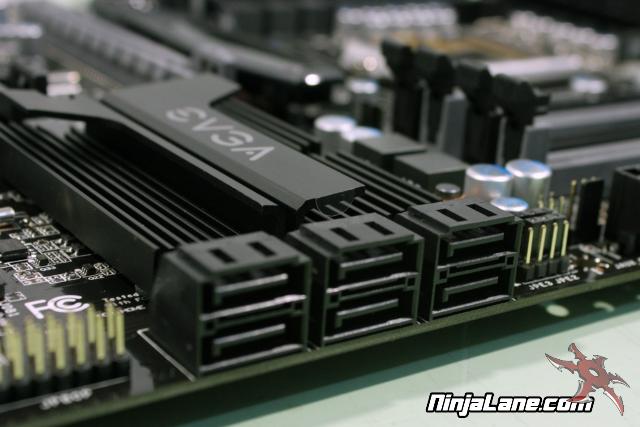
The EVGA P55 FTW is a SATA only motherboard meaning that you will not find any legacy IDE connections on board. The P55 Southbridge supports up to 6 SATA connectors at 3.0Gb/s speed. You'll find these located near the bottom edge of the board at 90 degree angles to help with cable management, and avoiding issues with large graphic cards.
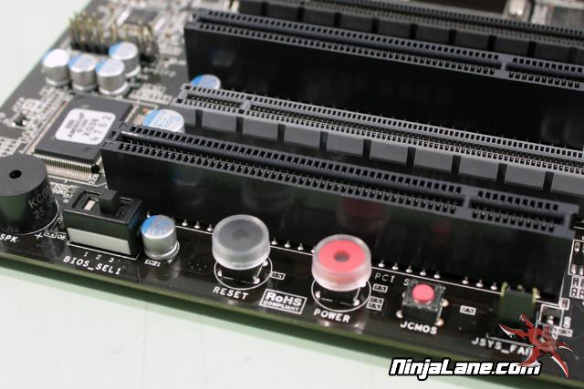
The Power/Reset buttons are located under the last PCI slot and are great when using this motherboard on a test bench, just don't expect easy access after the board has been installed. To the right of the Power/Reset you will find the CMOS clear button, an important feature when overclocking. To the left you will find a 3 position BIOS select switch.
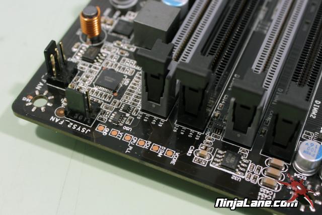
Overclockers will enjoy this next feature, voltage test points so you can verify each of the critical voltages externally with your own meter. There are many reasons for this; the biggest one is related to variances in component resistance that will throw off the software monitors and give you inaccurate readings.
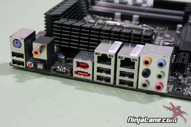
The back panel is quite full and features the following. 6x USB 2.0 connectors, 1x e-SATA port, 1x USB 2.0/e-SATA hybrid port, 2x Gigabit Lan, 1x Firewire(IEEE1394a), 6-channel sound is supported with Analog, Optical, or Coaxial connections.
A legacy PS/2 keyboard port is available along with a Clear CMOS button nearby.
A legacy PS/2 keyboard port is available along with a Clear CMOS button nearby.
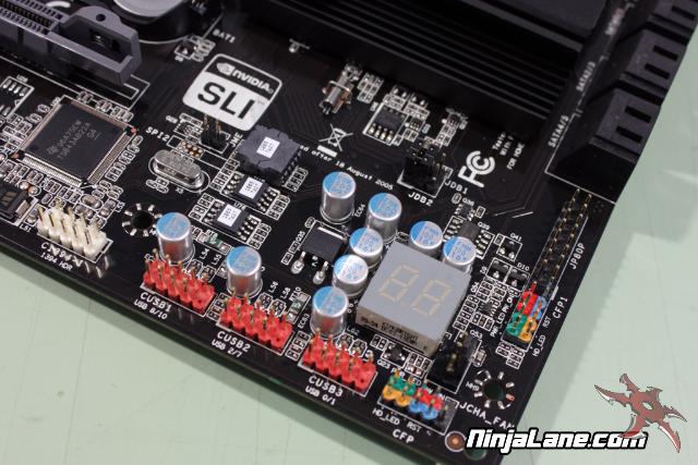
The front panel connector section of the motherboard is pretty typical. Here you have access to the onboard IEEE1394 connections as well as 6 extra USB ports, ECP V2 header, and handy debug LED. The debug LED doubles as a temperature readout after the system has completely gone thru its posting process.
The EVGA P55 FTW is a multi BIOS motherboard complete with three independent BIOS chips. 2 are soldered to the motherboard while the 3rd is removable for manual swapping and hot-flashes. This just might be overkill, but there is no such thing as overkill in the enthusiast arena. EVGA has everyone covered and wants them to feel safe while messing with their BIOS testing and tuning.