After careful consideration I have decided to transfer all hardware review activities to a new domain. I purchased Hardwareasylum.com in 2012 and have been working hard to build a new and improved Ninjalane on that domain. If you are reading this you have reached one of the archived articles, news, projects and/or reviews that were left behind during the site migration.
Please update your bookmarks and be sure to visit the new and improved Ninjalane at Hardwareasylum.com
Sapphire Radeon HD 6950 Video Card Review
Author: Dennis Garcia
Published: Wednesday, December 15, 2010
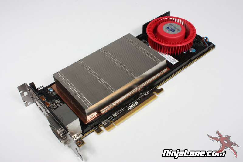
The Card Uncovered
While most people in the market for this card will simply install the card and enjoy the experience there are a select few that will want to modify the card to their liking. PCB modifications, extreme cooling, and water cooling are all popular with the enthusiast community and will require direct access to the PCB.
Below is what you will expect to see.
Removing the heatsink shroud is the first step and requires a delicate touch and access to 8 plastic tabs located across the top and bottom of the card. (btw one is hidden).
Below is what you will expect to see.
Removing the heatsink shroud is the first step and requires a delicate touch and access to 8 plastic tabs located across the top and bottom of the card. (btw one is hidden).
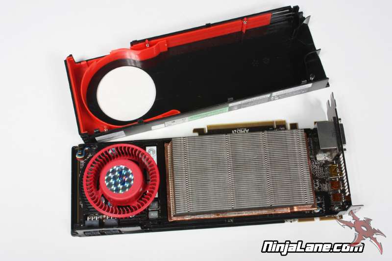
Once the shroud has been removed you'll see the basic heatsink and squirrel cage blower. The heatsink is a thin fin design sitting atop of a large vapor chamber. (eg flattened heatpipe).
To remove the heatsink you'll need to remove all of the screws on the back side of the card. Be sure to leave the 4 around the GPU until last. Once all of the screws have been removed you can lift way the heatsink assembly to expose the PCB. We used a wide flat screwdriver to pop the heatsink loose, whatever method you choose pay careful attention to the board components before you begin your operation.
To remove the heatsink you'll need to remove all of the screws on the back side of the card. Be sure to leave the 4 around the GPU until last. Once all of the screws have been removed you can lift way the heatsink assembly to expose the PCB. We used a wide flat screwdriver to pop the heatsink loose, whatever method you choose pay careful attention to the board components before you begin your operation.
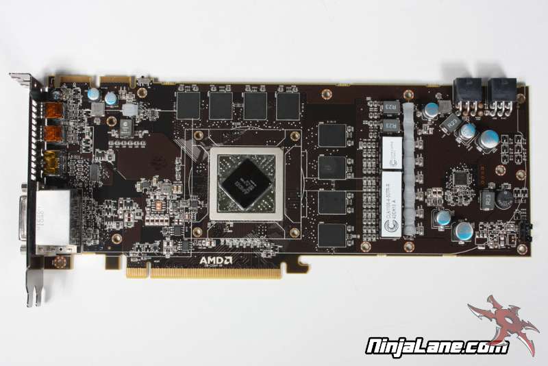
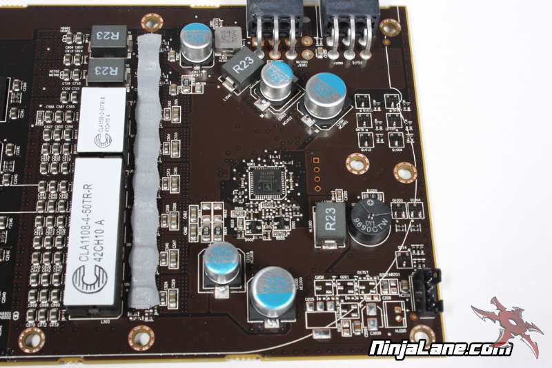
Overalls of the card, both front and back. You may notice the distinct lack of surface components. Almost makes you think this card is big only so they can use an oversized heatsink.
Here is a close up of the Crossfire bridge connectors and BIOS microswitch. As you can see the switch is either on or off. (on being the default setting)
Here is a close up of the Crossfire bridge connectors and BIOS microswitch. As you can see the switch is either on or off. (on being the default setting)
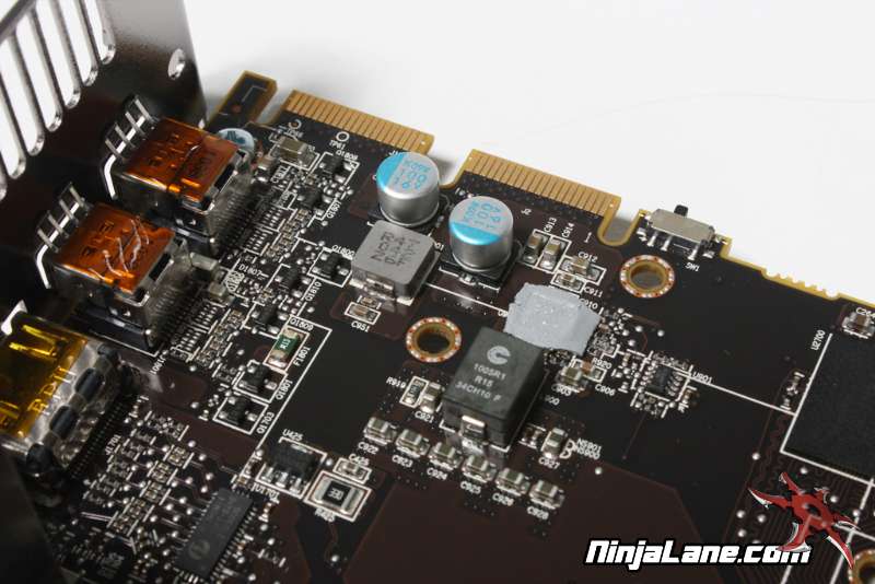
Here we have various components at the lower front of the PCB.
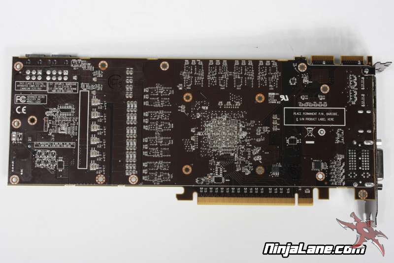
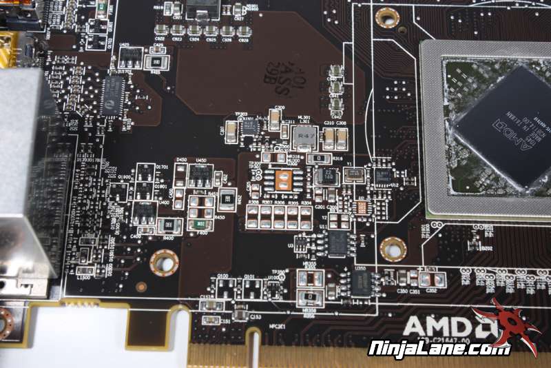
The back of the board is typically where the voltage regulators can be found. Some interesting things to notice would be the 2 extra power leads that are not hooked up and the vertical line of mosfets flanked by 2 mounting holes. The extra power connections indicates this PCB could in fact be similar (if not the same) as the 6970, and well, the mosfet position is just nice for aftermarket cooling options.
The back of the board is typically where the voltage regulators can be found. Some interesting things to notice would be the 2 extra power leads that are not hooked up and the vertical line of mosfets flanked by 2 mounting holes. The extra power connections indicates this PCB could in fact be similar (if not the same) as the 6970, and well, the mosfet position is just nice for aftermarket cooling options.
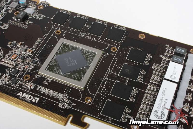
GPU and memory can be found in their normal arrangement with memory chips located on one side of the board only. The GPU mounting pattern is typical for AMD systems so those of you with individual waterblocks (like the Danger Den Maze 5) should have no issues getting them installed.